PVD layers transferred with a laser show remarkable "nano effects"
In recent months we have been intensively researching new layer properties that are made possible by our innovative laser-induced PVD coating technology ARA-LT®. We look forward to presenting the exciting results of our research to you.
Part 1: Porous silicon - structural and optical features
Starting with amorphous silicon that has been sputtered or vapor-deposited onto a PET film, layer modifications can be produced using a standard marking laser whose unusual and interesting properties open up completely new possibilities and signify substantial improvements for many fields of application.
The principle of these “laser coatings”, which we developed ourselves and offer under the ARA-LT® brand, can be described in simplified terms as follows: When a pulsed laser beam hits the PVD layer, a lot of energy is absorbed in a very short time locally very limited layer surface, which leads to an "explosive" liquefaction of the PVD layer, which is then transferred in the form of very many, very small droplets from the carrier surface to the product surface and solidifies there again.
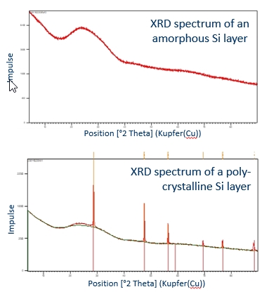
Depending on how the laser parameters are set, the crystal structure, optical properties and electrical conductivity can be specifically adjusted, for example, starting from one and the same silicon laser foil. In the "Crystal Structure" image, an XRD spectrum is shown at the top, which shows a sputtered, amorphous silicon layer, and the XRD spectrum at the bottom shows the sharp reflections of a polycrystalline layer - this is the silicon layer "lased" onto glass .
If the transmission spectra of this amorphous and the polycrystalline silicon layer, a few hundred nanometers thick, are recorded (picture "Transmission spectra"), then it can be seen that the laser-induced layer transfer results in the "silicon-typical" high transmission at longer wavelengths reduced to a maximum value of 3% over the entire wavelength range. For solar cells, for example, this means that on the one hand significantly less silicon is required to obtain a high interaction rate with photons and on the other hand the entire solar spectrum can be used (which should of course increase the efficiency significantly).
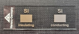
In the photo "Silicon on glass" two rectangles made of pure silicon are lasered. The surface of both rectangles is very porous. The one on the left (brown) is completely insulating and the one on the right (grey) has a conductivity five orders of magnitude higher than the literature value. This indicates that under the "special conditions" during the formation of the layer, i.e. during the laser-induced transfer, the electronic structure is also changed substantially - simply by different selected laser parameter settings.
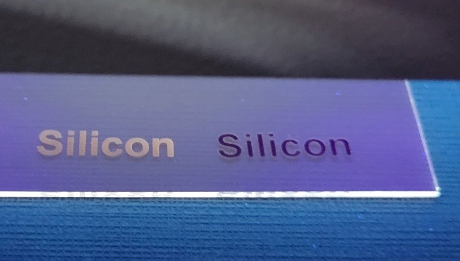
The (diffuse) color of silicon can also be "adjusted" under UV light, as the following photo shows:
In Part 2, which will be published shortly, we will report on the permanent catalytic activity and the "capillary effect without a capillary" of lasered, very porous silicon layers.
We look forward to interested partners with whom we can jointly develop new products or improve product properties.